Semiconductor manufacturing is a highly intricate process, comprising numerous steps and stages, with each one presenting the potential for contamination. Contamination in this context can be particularly costly, leading to yield losses and time wastage. To address these challenges, Real-Time Monitoring Systems offer a powerful solution, providing immediate detection and enabling rapid mitigation in potential yield losses. In this blog post, we will delve into the role of liquid contamination in semiconductor manufacturing and explore how Real-Time Monitoring Systems can effectively manage this crucial aspect of production.
Did you know that water is one of the most critical process tools in semiconductor wafer fabrications processes?
By the late 2010s and early 2020s, leading-edge fabs use between 2,000 to 3,000 liters of Ultra Pure Water (UPW) per 300mm wafer.
The Complex Process of Semiconductor Manufacturing
A typical semiconductor manufacturing facility, often referred to as a wafer fab, is where integrated circuits (ICs) are created. This process involves a myriad of steps, and it is essential that the products remain free from contamination. Unmonitored contamination can significantly impact product yield and quality.
Semiconductor manufacturing involves the creation of multiple copies of an integrated circuit on a single silicon wafer. This process includes the formation of numerous patterned layers both on and within the substrate, ultimately resulting in a fully functional integrated circuit. Throughout this complex process, control of contamination is paramount, specifically focusing on particulate contamination.
The First Step: Wafer Production
The journey of semiconductor manufacturing begins with the production of silicon wafers. These wafers are thin, round slices of semiconductor material, primarily silicon, and serve as the foundation for integrated circuits. The process begins with purified polycrystalline silicon, which is heated to a molten liquid state. A small solid silicon seed is introduced into the molten liquid, and as it is gradually pulled from the melt, a single crystal ingot forms. This crystal ingot is then further processed to create uniform-diameter wafers.
Wafer Fabrication: A Cleanroom Journey
The heart of semiconductor manufacturing lies in the wafer fabrication facility, where the actual integrated circuit is formed on and within the wafer. The fabrication process takes place within a cleanroom environment and involves a series of key steps:
1. Thermal Oxidation or Deposition
In this step, wafers are pre-cleaned using high-purity, low-particulate chemicals. This cleaning process is essential to ensure high-yield products. The silicon wafers are exposed to ultrapure oxygen in diffusion furnaces, forming a uniform silicon dioxide film on the wafer’s surface.
2. Masking (Photolithography)
Masking is a critical step in semiconductor manufacturing, protecting one area of the wafer while work is performed on another. A light-sensitive film, known as photoresist, is applied to the wafer’s surface. A photo aligner aligns the wafer with a mask and projects intense light through it, exposing the photoresist with the desired pattern. Precise alignment is crucial for this process.
3. Etching
The etching process involves the removal of areas not protected by the hardened photoresist. Chemical solutions or plasma are used to etch away the exposed portions. Careful inspection follows to ensure correct image transfer from the mask to the top layer.
4. Doping
Doping introduces atoms with either one electron less or one electron more than silicon, altering the silicon’s electrical characteristics. These regions are labeled P-type or N-type based on their conducting properties.
These processes are repeated several times until all active devices are formed on the wafer. Afterward, dielectric deposition and metallization steps are employed to interconnect the individual devices. Each level of interconnect is separated by dielectric layers.
Liquid Contamination Monitoring and Control
Contamination control in semiconductor manufacturing primarily focuses on particulate contamination. Managing liquid contamination is critical at various stages of the process. Here are some key aspects of liquid contamination monitoring and control:
1. Chemical Quality
In the initial stages of wafer fabrication, chemicals are used for pre-cleaning and other processes. It is essential to monitor these chemicals for particulate contamination to prevent introducing contaminants into the manufacturing process. Liquid particle counters are valuable tools for monitoring the cleanliness of these chemicals.
2. Gas Quality
The etching process involves the use of gases, and monitoring gas quality is crucial to prevent gas-related contamination. Gas suppliers typically provide certificates indicating gas purity. However, conducting in-house monitoring of gas batches can provide an added layer of assurance.
3. Operator Contamination
Despite strict cleanroom protocols and attire, cleanroom operators can inadvertently introduce particulate contamination. Monitoring the points where operators interact with wafers is essential to ensure a clean working environment. Air particle counters can help track any particulate shedding by operators.
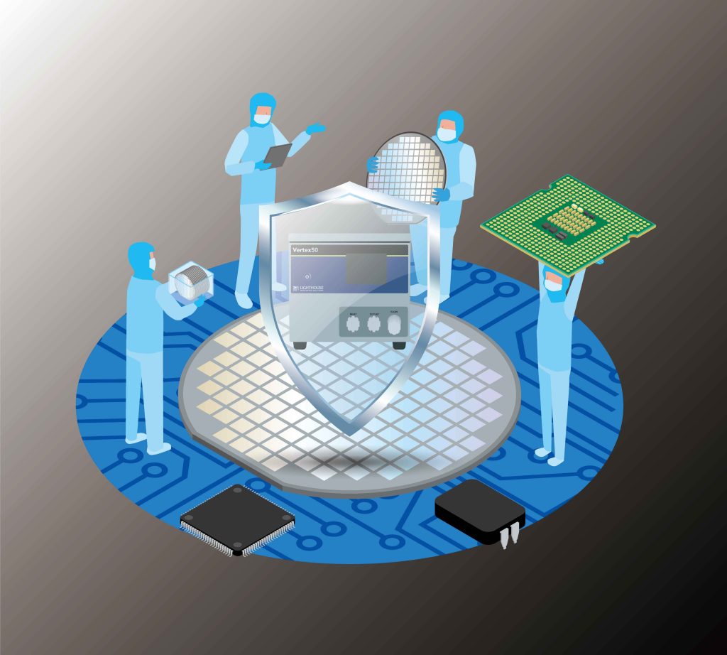
Real-Time Monitoring Systems: Defending Against Contamination
Real-Time Monitoring Systems play a pivotal role in safeguarding semiconductor manufacturing from contamination-related challenges. These systems offer immediate detection capabilities, allowing for swift mitigation actions to minimize the impact on yield and product quality. They focus on critical contamination control points in the production process, preserving the integrity of semiconductor products.
The Importance of Risk Assessment
Effective liquid contamination control in semiconductor manufacturing hinges on conducting comprehensive risk assessments. These assessments identify potential contamination sources, assess the severity of contamination consequences, evaluate the likelihood of contamination events, and calculate overall risk levels. By adopting a structured risk assessment approach, semiconductor manufacturers gain clarity on what and where to monitor for liquid contamination, simplifying the daunting task of contamination control.
The Critical Role of Yield Management
In semiconductor manufacturing, yield management is paramount. Line yield and defect density are closely guarded secrets, measuring the effectiveness of material handling, process control, and labor. Incremental increases in yield reduce manufacturing costs per wafer or per square centimeter of silicon. Contamination, particularly particulate contamination, can significantly impact yields in the era of device miniaturization and larger die sizes. Liquid Particle Counters play a critical role in ensuring that UPW is particulate free to ensure a contamination free process of the wafer.
In conclusion, liquid contamination control in semiconductor manufacturing is a complex challenge that demands careful attention. Real-Time Monitoring Systems, guided by risk assessments, serve as the frontline defense against liquid contamination. By adopting advanced monitoring solutions and stringent contamination control measures, semiconductor manufacturers can navigate the intricacies of the industry, maintain high yields, and produce top-tier products that power our modern world.